
Fluxless TCB vs TCB
As interconnection pitches shrink below 10µm for advanced logic and memory applications, fluxless TCB solves the issues that standard TCB encounters with the flux.
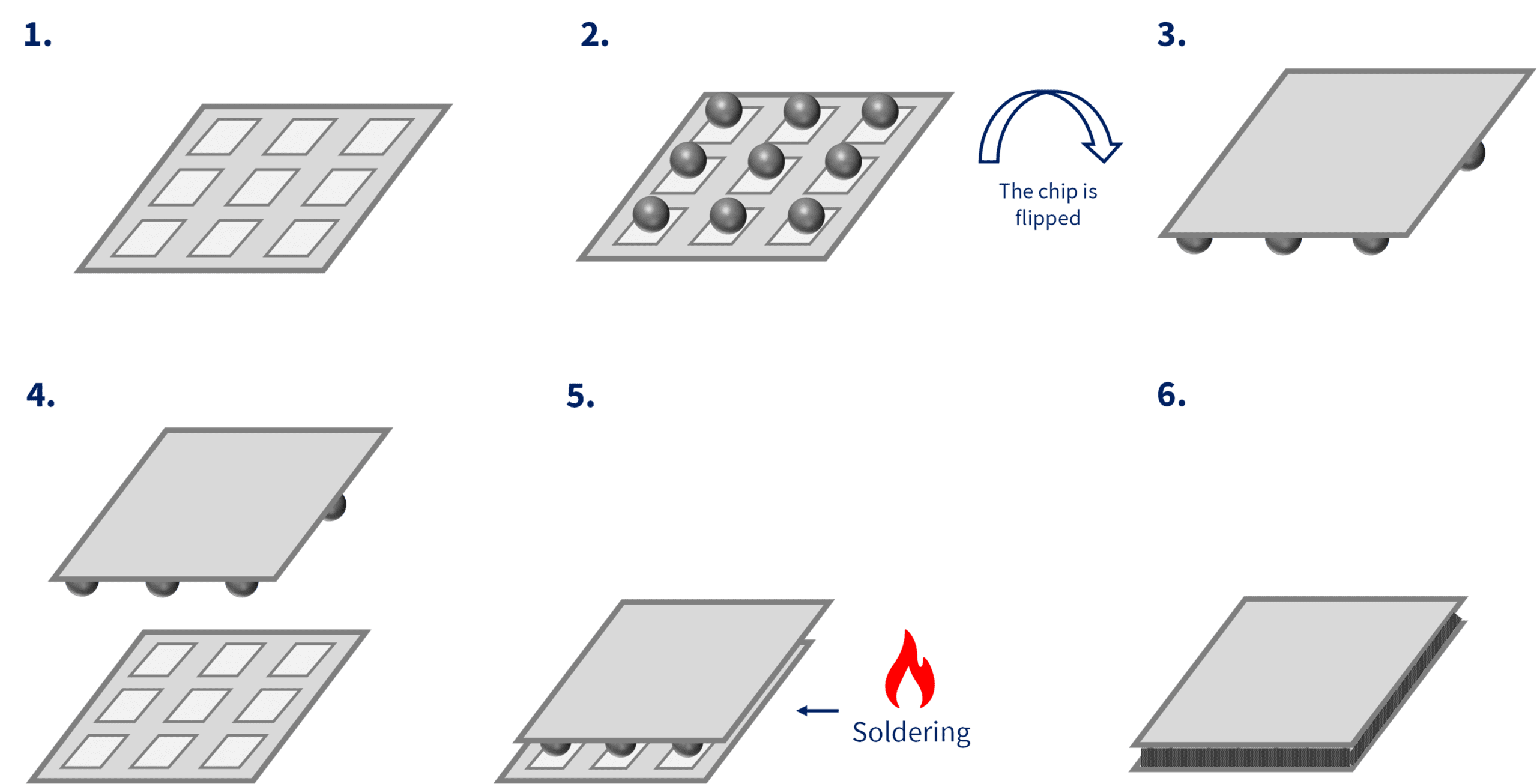
As interconnection pitches shrink below 10µm for advanced logic and memory applications, fluxless TCB solves the issues that standard TCB encounters with the flux.

The front-end and back-end are highly interdependent. A constant feedback loop between front and back-end engineers is necessary to improve manufacturing yields.
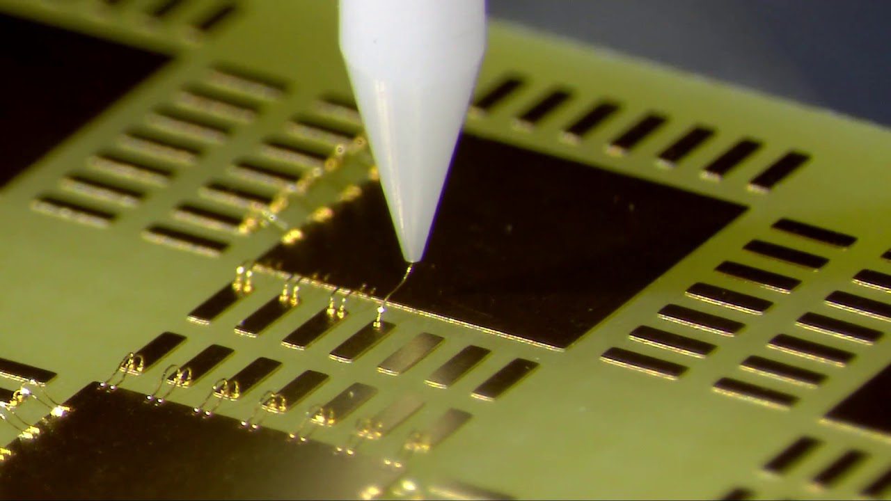
Wire bonding is a cheap and reliable semiconductor packaging method- Flip-chip is an advancement, creating more dense interconnections and allowing 3D vertical stacking.
Fab yield refers to the percentage of working chips in a semiconductor wafer. If a fab can’t meet the requirements, customers will switch to another