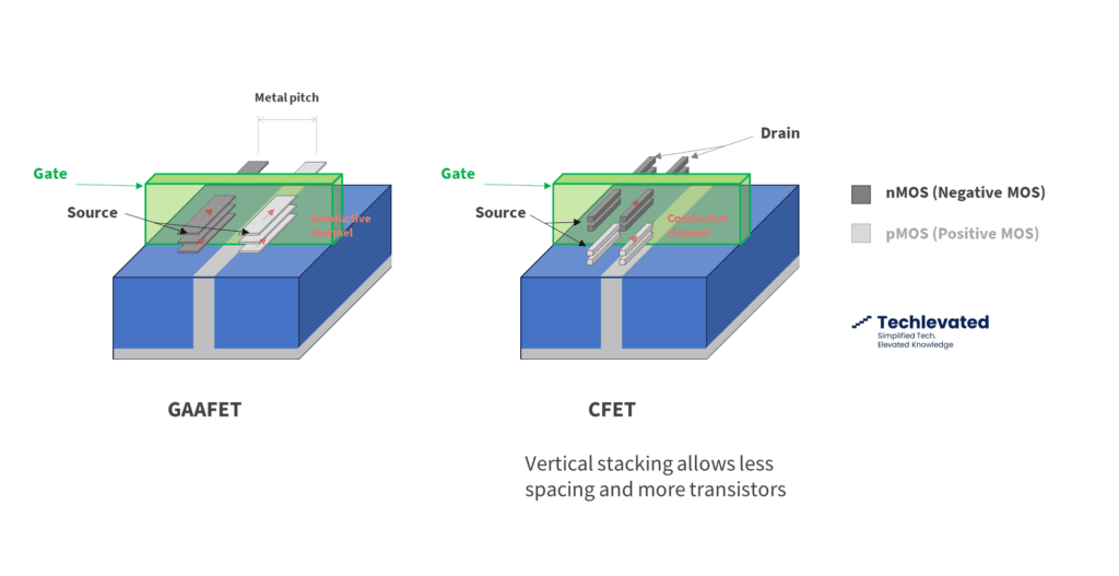
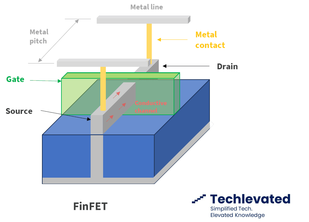
Table of Contents

The CFET Transistor: Shrinking Nodes Beyond 2030

Complementary FETs (CFET) are a potential evolution over Gate-All-Around FETs (GAAFET) semiconductor transistors. Let´s be clear on something first, when we talk about CFET transistors we talk about a technology that is not expected until beyond 2030 according to IMEC. GAAFET, its predecesor, is not expected to enter high-volume manufacturing (HVM) until 2025. CFETs will however mark a further advancement in multigate transistors, switching from horizontally stacked channels to vertically stacked ones. This will allow further shrinking of semiconductor patterns and the advancement of Moore´s Law.

Semiconductor transistors can be n-channels (nMOS or negative MOS) or p-channels (pMOS or positive MOS). These two type of channels act as logic gates that act in a complementary way. nMOS channel conducts with high voltage, while pMOS conducts with low voltage. In FinFET and GAAFET implementations, nMOS and pMOS transistors (gray and white in the image) are placed besides each other. However, reducing the metal pitch (the distance from one transistor´s gate to another) beyond 16nm is becoming increasingly difficult, as this has unintended consequences such as leakage current, increased power consumption and difficulties in maintaining control of the transistor when it is in off-state.

Switching To Vertically-Stacked Channels

That is why the industry might try to switch to vertically stacked transistors (CFETs, see image) instead of horizontally stacked ones (FinFETs and GAAFETs) in the future. The CFET maintains the gate-all-around structure (the transistor´s gate fully wraps the four faces of each ribbon), but instead of placing the NMOS and PMOS close to one another, it will stack them vertically. This way the used area is much smaller and allows for a much higher density of transistors, allowing further shrinking of semiconductor patterns and improvements in power, performance and area (PPA).

Designing CFETs will however have its own challenges. The etching process, which applies chemical substances to remove unnecessary materials from the wafer, will become more complex, as engineers must find a way to etch the top nMOS bands without hurting the bottom pMOS ones. Semiconductor design teams and foundries need to start working on a design 5 to 10 years ahead, as it takes a long time to bring R&D ideas into high-volume manufacturing. For example, GAAFETs have been talked by industry experts for more than a decade, but the first ICs using GAAFET will arrive in 2024, and it is not expected to reach high-volume manufacturing until 2025. This means it will still take take a while until CFETs become a reality.

Related Posts

Bandgap

SiC vs GaN Transistors

Silicon carbide (SiC) is used in electric vehicles due to its wide bandgap and great thermal conductivity. Gallium nitride (GaN) shares many characteristics with SiC while also minimizing RF noise.

Read More »