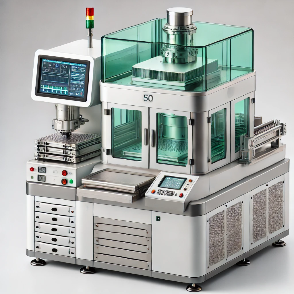
Fluxless TCB vs TCB
As interconnection pitches shrink below 10µm for advanced logic and memory applications, fluxless TCB solves the issues that standard TCB encounters with the flux.
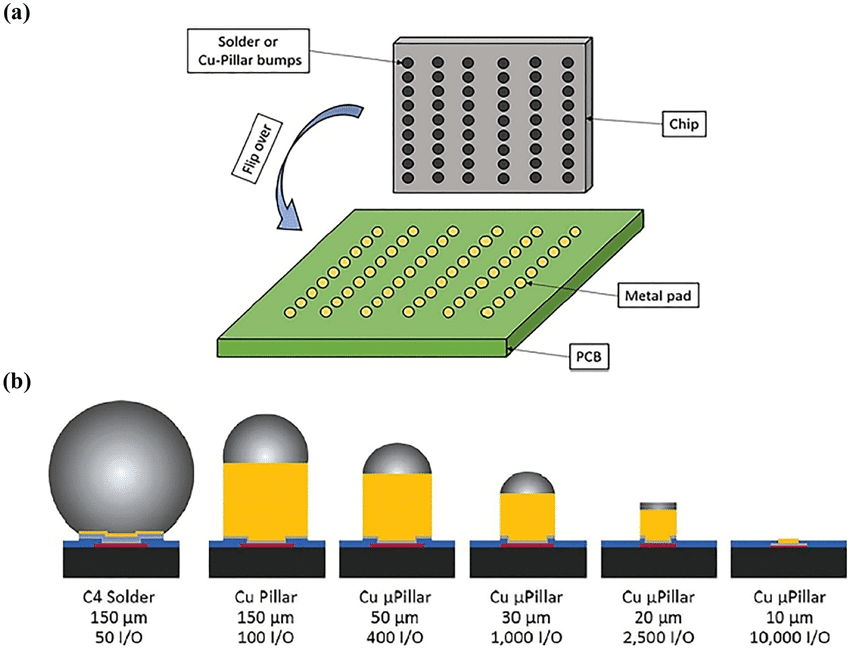
As interconnection pitches shrink below 10µm for advanced logic and memory applications, fluxless TCB solves the issues that standard TCB encounters with the flux.
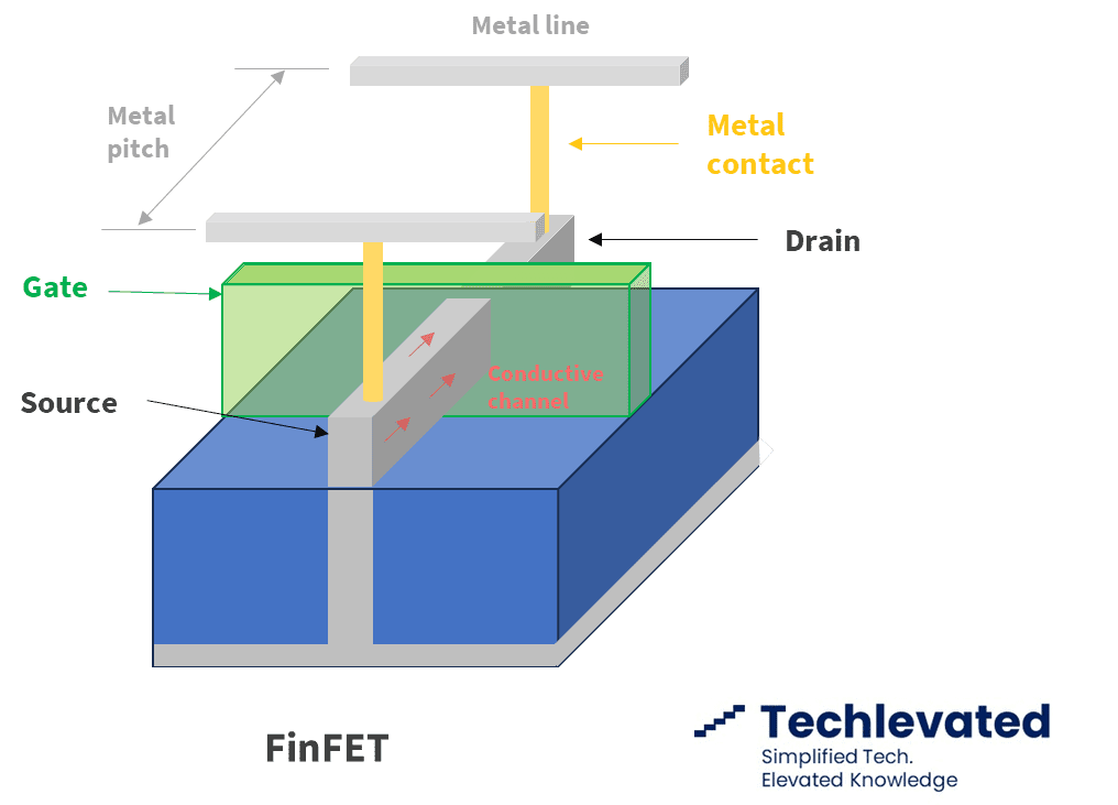
The metal pitch refers to the distance between the centers of two adjacent metal interconnect lines on an integrated circuit (IC). Since transistors evolved into 3D strucrures, this measurement has lost significance.
The front-end and back-end are highly interdependent. A constant feedback loop between front and back-end engineers is necessary to improve manufacturing yields.
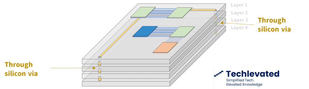
Built directly into the silicon, through silicon vias (TSV) facilitate 3D IC integration and allow for more compact packaging. They have become the default solution to interconnect different chip layers or to stack chips vertically.
Silicon carbide (SiC) is used in electric vehicles due to its wide bandgap and great thermal conductivity. Gallium nitride (GaN) shares many characteristics with SiC while also minimizing RF noise.
GPU vs CPU is a parallelization vs complexity dilemma. While GPUs can manage very large parallel calculations, they struggle with linear, more heterogeneous tasks, where CPUs excel.