Fluxless TCB vs TCB
As interconnection pitches shrink below 10µm for advanced logic and memory applications, fluxless TCB solves the issues that standard TCB encounters with the flux.
Tape out is the process in which the final design of a semiconductor chip is sent to the manufacturing facility for production. It marks the end of the design phase and the beginning of the manufacturing process. During the design phase, engineers create a detailed blueprint of the chip, including its architecture, circuitry, and layout.
Once the design is complete, it undergoes rigorous testing and verification to ensure that it functions correctly. This includes checking for any potential defects or issues that could affect the chip’s performance.
When the design has been thoroughly tested and verified, it is time for tape-out. This involves generating a set of electronic files that contain the precise instructions for fabricating the chip. These files specify the exact dimensions, materials, and structures that make up the chip, as well as the positioning and connections of the various components.
The tape-out files are then sent to a semiconductor manufacturing facility, or fab, where the actual fabrication process takes place. The fab uses these files as a guide to manufacture the chip on a silicon wafer, layer by layer, through processes like photolithography, etching, and deposition among others.
After the manufacturing process is complete, the chip undergoes further testing to ensure that it meets the required specifications and functions as intended. Once it passes these tests, it can be packaged and prepared for distribution to electronics manufacturers who integrate the chip into smartphones, PCs, or other electronic devices.
In the next section you can find a real life case study about the tape-out process, involving NVIDIA and TSMC.
NVIDIA Corporation is an American chip fabless company known for its graphics processing units (GPUs) and deep learning accelerators. In 2018 Nvidia developed and taped-out their Turing GPU.
Challenges:
Tape-Out Process:
Results: NVIDIA’s Turing GPU architecture, manufactured through TSMC, was a significant success. It introduced real-time ray tracing to gaming and marked a major leap in graphics and AI processing capabilities. The successful tape-out ensured that the complex design was translated into functional silicon, enabling NVIDIA to maintain its leadership in the GPU market.
This case study underscores the crucial role of the tape-out phase in semiconductor manufacturing. NVIDIA’s meticulous planning, validation, and collaboration with a trusted foundry (TSMC) were essential in ensuring the successful production of their Turing GPUs. It highlights the importance of precision and attention to detail during the tape-out process to achieve the desired product’s functionality and performance.
In the 1980s, the tape-out process was done manually and was a time-consuming and error-prone process. Designers would create artwork of the various layers of the chip using pen plotters, and these artworks would then be photographed onto film. In the 1990s, computer-aided design (CAD) tools began to automate the tape-out process. Designers could create digital versions of the chip artwork using software and these designs could be uploaded to the foundry directly.
The move to smaller process nodes (i.e. smaller transistors) at the beginning of the 20th century meant that the tape-out process became more complex. Designers needed to consider factors like power consumption, timing, and signal integrity in addition to the physical layout of the chip. More recently there has been a move towards “multi-project wafer” (MPW) services, where multiple designs from different customers are fabricated on a single wafer. This approach allows smaller companies and startups to get their designs fabricated at a lower cost.
Nowadays, the tape-out process is highly automated and uses sophisticated software tools to create and verify chip designs. Foundries typically offer a range of process options, from mature nodes optimized for cost and reliability to the latest cutting-edge technology nodes. The outcome of the fabrication is a packaged chip that can be used in a variety of electronic devices.

As interconnection pitches shrink below 10µm for advanced logic and memory applications, fluxless TCB solves the issues that standard TCB encounters with the flux.
The metal pitch refers to the distance between the centers of two adjacent metal interconnect lines on an integrated circuit (IC). Since transistors evolved into 3D strucrures, this measurement has lost significance.

The front-end and back-end are highly interdependent. A constant feedback loop between front and back-end engineers is necessary to improve manufacturing yields.

Built directly into the silicon, through silicon vias (TSV) facilitate 3D IC integration and allow for more compact packaging. They have become the default solution to interconnect different chip layers or to stack chips vertically.

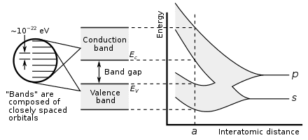
Silicon carbide (SiC) is used in electric vehicles due to its wide bandgap and great thermal conductivity. Gallium nitride (GaN) shares many characteristics with SiC while also minimizing RF noise.

GPU vs CPU is a parallelization vs complexity dilemma. While GPUs can manage very large parallel calculations, they struggle with linear, more heterogeneous tasks, where CPUs excel.