Fluxless TCB vs TCB
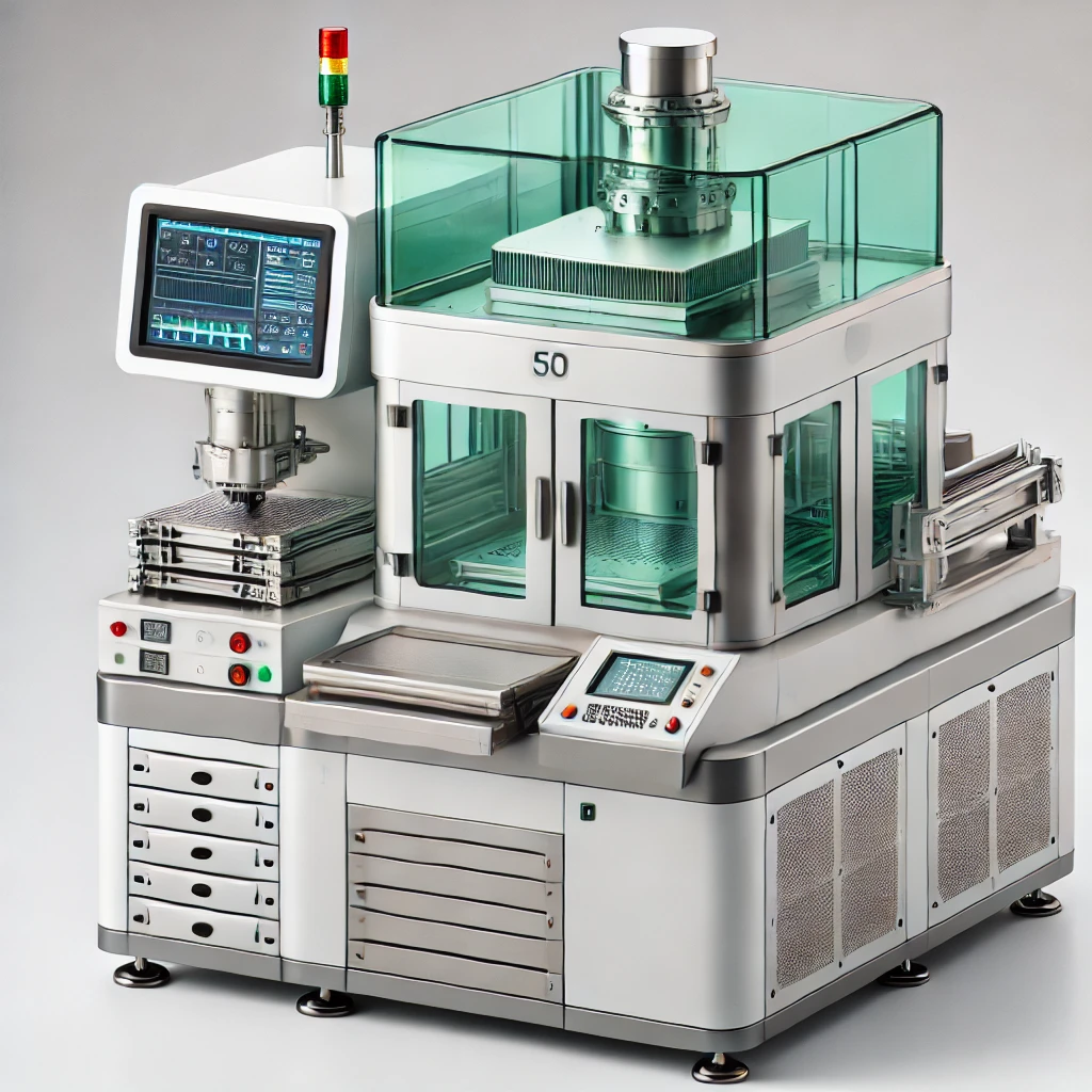
As interconnection pitches shrink below 10µm for advanced logic and memory applications, fluxless TCB solves the issues that standard TCB encounters with the flux.
Fowlp stands for Fan out wafer level packaging, which is a type of chip packaging technology in the semiconductor industry. While traditional packaging technologies such as system in package (SiP) and chip on board (COB) essentially place a single packaged chip onto a printed circuit board (PCB), FOWLP technology uses a wafer as the substrate for the packaging.
The concept of FOWLP originated from wafer level packaging (WLP), which was first introduced in the early 2000s. WLP soon became an attractive packaging option because of its small form factor, low cost, and compatibility with high volume manufacturing. However, the original WLP technology had some limitations such as I/O density and limited number of chips per wafer, which restricted its application range. In contrast, FOWLP technology overcomes most of these limitations by allowing chips to be directly connected in a redistributed layout at the wafer level using thin film redistribution layers.
In FOWLP, chips are first thinned and then placed on a reconstituted wafer, which contains a layer of polyimide or other insulating material to provide mechanical and electrical separation between chips. Redistribution layers (RDLs) are then added to connect the I/O of the chips to the outside world through metal vias that extend through the insulating layers. The RDLs, which are typically made of copper, are patterned using lithography to achieve the desired interconnect design.
The final step in FOWLP is to singulate the wafer into individual fan out packages. The singulation process involves dicing the wafer to create individual packages using a process known as sawing, laser cutting or stealth dicing. The resulting packages are then encapsulated and tested for functionality before being shipped to customers.
FOWLP technology has a number of advantages over traditional packaging technologies. First, FOWLP allows for higher I/O counts and smaller form factors than other package types. It also offers improved thermal and electrical performance, lower cost and shorter time to market as the technology eliminates the need for a separate printed circuit board (PCB) for the chip package. Finally, it supports heterogeneous integration, which allows chips of different sizes and functionality to be combined in one package, thus opening up new possibilities for system level integration.

As interconnection pitches shrink below 10µm for advanced logic and memory applications, fluxless TCB solves the issues that standard TCB encounters with the flux.
The metal pitch refers to the distance between the centers of two adjacent metal interconnect lines on an integrated circuit (IC). Since transistors evolved into 3D strucrures, this measurement has lost significance.

The front-end and back-end are highly interdependent. A constant feedback loop between front and back-end engineers is necessary to improve manufacturing yields.

Built directly into the silicon, through silicon vias (TSV) facilitate 3D IC integration and allow for more compact packaging. They have become the default solution to interconnect different chip layers or to stack chips vertically.

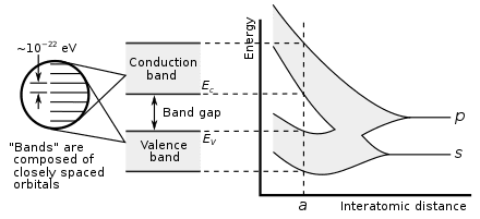
Silicon carbide (SiC) is used in electric vehicles due to its wide bandgap and great thermal conductivity. Gallium nitride (GaN) shares many characteristics with SiC while also minimizing RF noise.

GPU vs CPU is a parallelization vs complexity dilemma. While GPUs can manage very large parallel calculations, they struggle with linear, more heterogeneous tasks, where CPUs excel.